Readings Newsletter
Become a Readings Member to make your shopping experience even easier.
Sign in or sign up for free!
You’re not far away from qualifying for FREE standard shipping within Australia
You’ve qualified for FREE standard shipping within Australia
The cart is loading…


This title is printed to order. This book may have been self-published. If so, we cannot guarantee the quality of the content. In the main most books will have gone through the editing process however some may not. We therefore suggest that you be aware of this before ordering this book. If in doubt check either the author or publisher’s details as we are unable to accept any returns unless they are faulty. Please contact us if you have any questions.
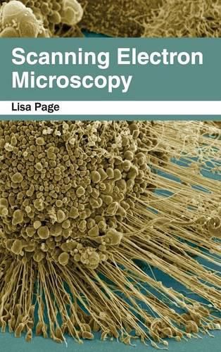
Fine focused electron and ion beams constitute(s) an inevitable part of methods and instruments employed in various science fields. SEMs are well instrumented and supplemented with advanced techniques and methods and thereby present endless possibilities in the areas of quantitative measurement of object topologies, surface imaging, performing elemental analysis and local electrophysical characteristics of semiconductor structures. Creation of micro and nanostructures involves extensive use of fine focused e-beam. This book focuses on various issues concerned with scanning electron microscopy, covering both theoretical and practical aspects. Numerous topics are organized under two sections, Material Science and Nanostructured Materials for Electronic Industry. This book includes contributions by renowned researchers and experts in this field.
$9.00 standard shipping within Australia
FREE standard shipping within Australia for orders over $100.00
Express & International shipping calculated at checkout
This title is printed to order. This book may have been self-published. If so, we cannot guarantee the quality of the content. In the main most books will have gone through the editing process however some may not. We therefore suggest that you be aware of this before ordering this book. If in doubt check either the author or publisher’s details as we are unable to accept any returns unless they are faulty. Please contact us if you have any questions.
Fine focused electron and ion beams constitute(s) an inevitable part of methods and instruments employed in various science fields. SEMs are well instrumented and supplemented with advanced techniques and methods and thereby present endless possibilities in the areas of quantitative measurement of object topologies, surface imaging, performing elemental analysis and local electrophysical characteristics of semiconductor structures. Creation of micro and nanostructures involves extensive use of fine focused e-beam. This book focuses on various issues concerned with scanning electron microscopy, covering both theoretical and practical aspects. Numerous topics are organized under two sections, Material Science and Nanostructured Materials for Electronic Industry. This book includes contributions by renowned researchers and experts in this field.