Readings Newsletter
Become a Readings Member to make your shopping experience even easier.
Sign in or sign up for free!
You’re not far away from qualifying for FREE standard shipping within Australia
You’ve qualified for FREE standard shipping within Australia
The cart is loading…


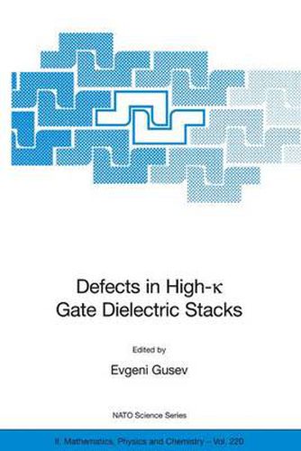
The goal of this NATO Advanced Research Workshop (ARW) entitled Defects in Advanced High-k Dielectric Nano-electronic Semiconductor Devices , which was held in St. Petersburg, Russia, from July 11 to 14, 2005, was to examine the very complex scientific issues that pertain to the use of advanced high dielectric constant (high-k) materials in next generation semiconductor devices. The special feature of this workshop was focus on an important issue of defects in this novel class of materials. One of the key obstacles to high-k integration into Si nano-technology are the electronic defects in high-k materials. It has been established that defects do exist in high-k dielectrics and they play an important role in device operation. However, very little is known about the nature of the defects or about possible techniques to eliminate, or at least minimize them. Given the absence of a feasible alternative in the near future, well-focused scientific research and aggressive development programs on high-k gate dielectrics and related devices must continue for semiconductor electronics to remain a competitive income producing force in the global market.
$9.00 standard shipping within Australia
FREE standard shipping within Australia for orders over $100.00
Express & International shipping calculated at checkout
The goal of this NATO Advanced Research Workshop (ARW) entitled Defects in Advanced High-k Dielectric Nano-electronic Semiconductor Devices , which was held in St. Petersburg, Russia, from July 11 to 14, 2005, was to examine the very complex scientific issues that pertain to the use of advanced high dielectric constant (high-k) materials in next generation semiconductor devices. The special feature of this workshop was focus on an important issue of defects in this novel class of materials. One of the key obstacles to high-k integration into Si nano-technology are the electronic defects in high-k materials. It has been established that defects do exist in high-k dielectrics and they play an important role in device operation. However, very little is known about the nature of the defects or about possible techniques to eliminate, or at least minimize them. Given the absence of a feasible alternative in the near future, well-focused scientific research and aggressive development programs on high-k gate dielectrics and related devices must continue for semiconductor electronics to remain a competitive income producing force in the global market.