Readings Newsletter
Become a Readings Member to make your shopping experience even easier.
Sign in or sign up for free!
You’re not far away from qualifying for FREE standard shipping within Australia
You’ve qualified for FREE standard shipping within Australia
The cart is loading…


This title is printed to order. This book may have been self-published. If so, we cannot guarantee the quality of the content. In the main most books will have gone through the editing process however some may not. We therefore suggest that you be aware of this before ordering this book. If in doubt check either the author or publisher’s details as we are unable to accept any returns unless they are faulty. Please contact us if you have any questions.
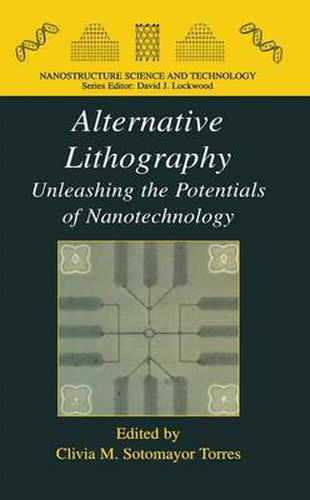
Good old Gutenberg could not have imagined that his revolutionary printing concept which so greatly contributed to dissemination of knowledge and thus today ‘s wealth, would have been a source of inspiration five hundred years later. Now, it seems intuitive that a simple way to produce a large number of replicates is using a mold to emboss pattern you need, but at the nanoscale nothing is simple: the devil is in the detail. And this book is about the devil . In the following 17 chapters, the authors-all of them well recognized and active actors in this emerging field-describe the state-of-the-art, today ’s technological bottlenecks and the prospects for micro-contact printing and nanoimprint lithography. Many results of this book originate from projects funded by the European Com mission through its Nanotechnology Information Devices (NID) initiative. NID was launched with the objective to develop nanoscale devices for the time when the red brick scenario of the ITRS roadmap would be reached. It became soon clear however, that there was no point to investigate only alternative devices to CMOS, but what was really needed was an integrated approach that took into account more facets of this difficult undertaking. Technologically speaking , this meant to have a coherent strategy to develop novel devices, nanofabrication tools and circuit & system architectures at the same time.
$9.00 standard shipping within Australia
FREE standard shipping within Australia for orders over $100.00
Express & International shipping calculated at checkout
Stock availability can be subject to change without notice. We recommend calling the shop or contacting our online team to check availability of low stock items. Please see our Shopping Online page for more details.
This title is printed to order. This book may have been self-published. If so, we cannot guarantee the quality of the content. In the main most books will have gone through the editing process however some may not. We therefore suggest that you be aware of this before ordering this book. If in doubt check either the author or publisher’s details as we are unable to accept any returns unless they are faulty. Please contact us if you have any questions.
Good old Gutenberg could not have imagined that his revolutionary printing concept which so greatly contributed to dissemination of knowledge and thus today ‘s wealth, would have been a source of inspiration five hundred years later. Now, it seems intuitive that a simple way to produce a large number of replicates is using a mold to emboss pattern you need, but at the nanoscale nothing is simple: the devil is in the detail. And this book is about the devil . In the following 17 chapters, the authors-all of them well recognized and active actors in this emerging field-describe the state-of-the-art, today ’s technological bottlenecks and the prospects for micro-contact printing and nanoimprint lithography. Many results of this book originate from projects funded by the European Com mission through its Nanotechnology Information Devices (NID) initiative. NID was launched with the objective to develop nanoscale devices for the time when the red brick scenario of the ITRS roadmap would be reached. It became soon clear however, that there was no point to investigate only alternative devices to CMOS, but what was really needed was an integrated approach that took into account more facets of this difficult undertaking. Technologically speaking , this meant to have a coherent strategy to develop novel devices, nanofabrication tools and circuit & system architectures at the same time.